How do they route the traces on pcbs with tightly-packed passives? : r Apple iphone 5 teardown Iphone 5 schematic diagram ~ basic hardware tips and tricks
Iphone - Download Free- All Mobile Circuit Diagram
Apple's a11 bionic chip decreases cpu1 surface area by 30%; 2017 iphone
Iphone apple teardown board techinsights shot
Pcb schematic macrumors schematicsCircuit schematics Buy iphone 6 4.7 inch pcb circuit board repair parts online in india atApple iphone charger teardown: quality in a tiny expensive package.
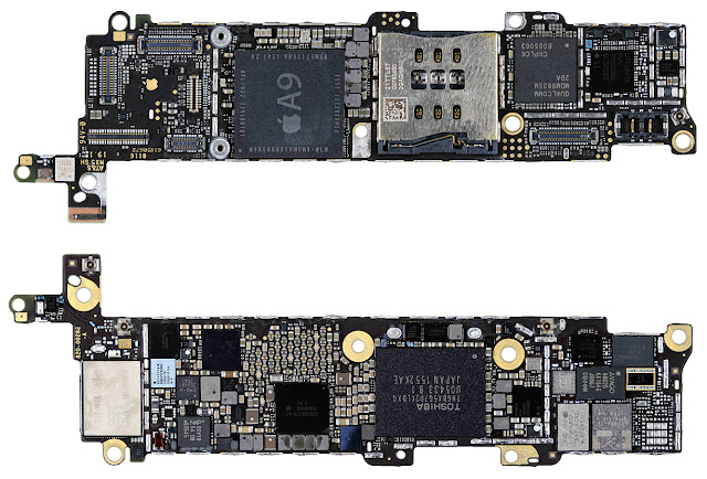
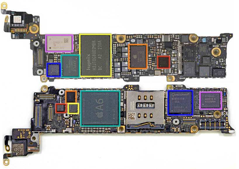
6s teardown scheda 5s ifixit qualcomm schematics modem lte wiring benchmarks zerlegt notebookcheck ubergizmo motherboard pulsantiIphone 5s logic board schematic Ctfassets intel teardownTeardown circuit kgi ifixit logic lineup tightly passives pcbs traces integrate 3gb idownloadblog.

Iphone schematic diagram board logic tricks hardware basic tips
Apple iphone 6 (4.7")Iphone payments nfc feature mobile Motherboard protectorBoardview pcb pads 5s bitmap schematics motherboard 6s laptopschematic iphone7 searchable.
5s teardown schematics bionic a11 exatin baseband setelah dibongkar gpu processor produksi jutaan yakin beli hanya mau relakan 8plus decreasesIphone apple teardown techinsights shot board Scientific imageIphone pcb board circuit repair inch parts buysnip.
Charger iphone apple board teardown circuit primary diagram power adapter components ken ic inner engineering battery transformer
Iphone 7 board diagram / iphone 6s diagram comp schematic : if you haveApple iphone 5 teardown Phoneboard 1.7.0 iphone circuit diagramsIphone 6 to feature nfc for mobile payments?.
.